- Ziva@CKlasersz.com
- WeChat:86-13138536413
- 400-168-9906
- 0755 27084852
- 3201809842@qq.com
- WeChat:86-19879133659
- 3376937209@qq.com
- WeChat:86-189 8489 0902


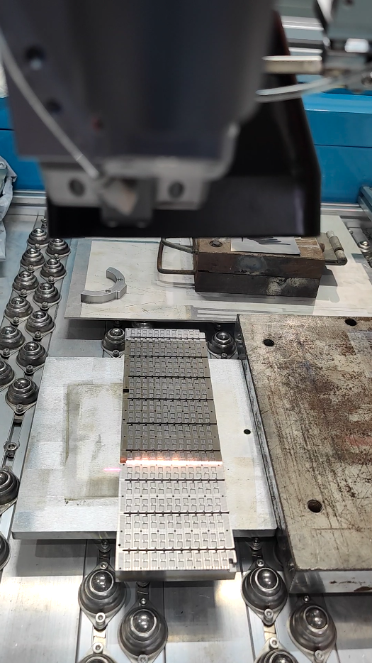
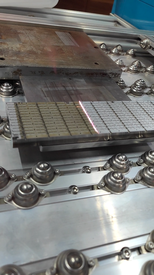
Application Object: Semiconductor packaging mold (IC molding mold) Main Contaminants: EMC epoxy molding compound residue, fine particle dust, oil stains, oxide layer and aging release agent Cleaning Difficulties: The mold cavity is tiny and precise. The dimensional tolerance of cavity and inserts is extremely strict. Traditional cleaning methods such as sandblasting and chemical soaking easily scratch and damage the coating, cause dimensional deviation, and directly affect the yield of chip packaging. Cleanliness requirements for semiconductor workshops are very high, and secondary pollution must be avoided. Advantages of Laser Cleaning
✅ Non-contact precision cleaning, protects precision cavity and plating layer without changing mold accuracy
✅ Dry process without chemicals, dust-free, suitable for semiconductor clean room standards
✅ Automatic alignment cleaning, works for narrow gaps and complex micro cavities
✅ Fast removal of molding residue, reduces mold maintenance downtime and improves production yield ✅ Stable and repeatable cleaning effect, easy to integrate into automated production lines
✅ No consumables, lower long-term maintenance cost compared with traditional cleaning