- Ziva@CKlasersz.com
- WeChat:86-13138536413
- 400-168-9906
- 0755 27084852
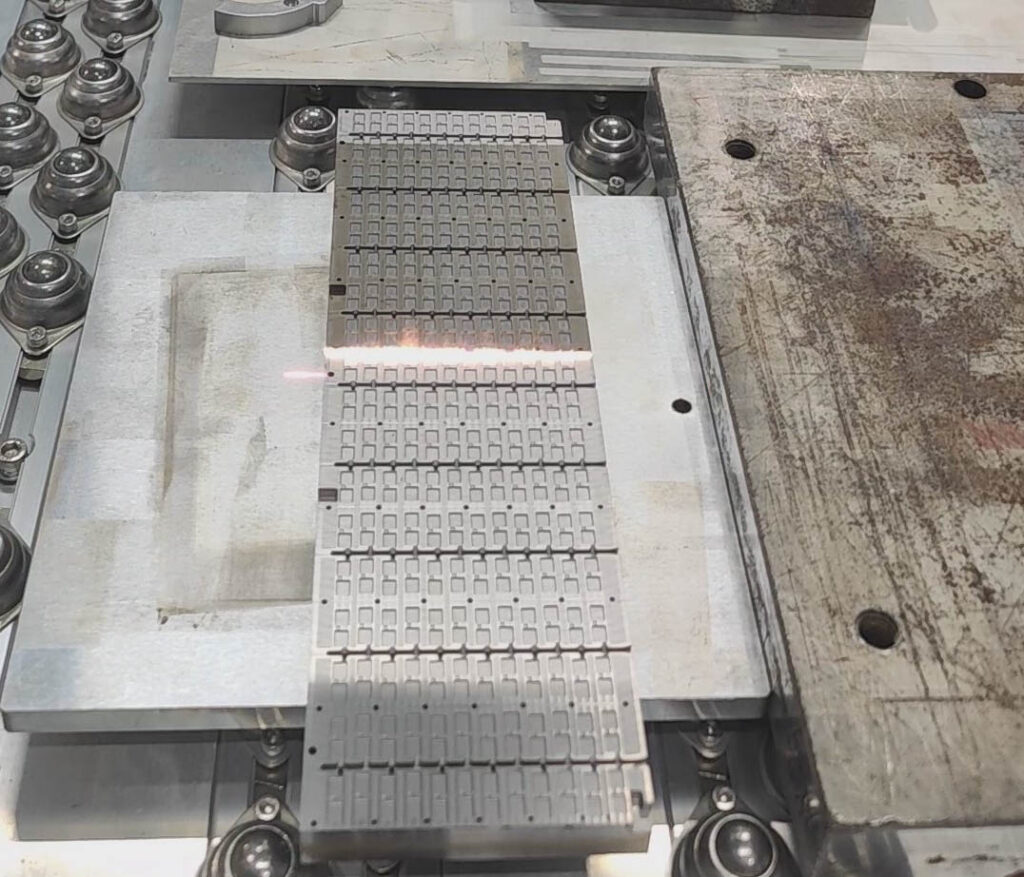
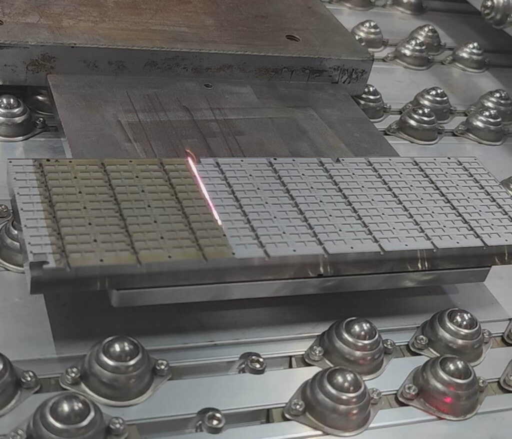
激光清洁具体应用:
A. 环氧模塑化合物残留物
这是最常见的污染物。在转注成型过程中,环氧模塑化合物(EMC)会在模具分型面、型腔拐角处和顶针孔上形成坚硬的碳化残留物。这些残留物含有硅粉等填料,非常难以清除。.
B. 脱模剂积累
用于确保脱模顺畅的脱模剂在高温下会持续碳化,在模具表面形成一层难以去除的绝缘膜,从而影响成型产品的表面质量和脱模性能。.
C. 无机污染物
金属闪光:这是由于成型材料中的杂质或模具轻微磨损所致。.
氧化层:这是模具在高温环境下长期使用后形成的表面氧化层。.
优势尺寸:
- 极致洁净,零二次污染:“干式”清洗可彻底清除任何残留介质。清洗后,模具表面洁净如新,从源头上杜绝了因清洗而引入的二次污染(如化学残留物和介质颗粒)。.
B. 提高芯片产品的良率和可靠性。通过实现100%标准下一致且无残留的清洗效果,该系统彻底消除了因模具污染导致的芯片粘接不良、翘曲、裂纹、气孔和点蚀等缺陷,从而直接提高了产品良率和长期可靠性。.
C. 满足绝对无尘环境的要求。该设备可完全集成到自动化生产线上,并在部分真空罩内运行。配合真空系统使用,可满足芯片制造对高标准洁净室的要求。.