- Ziva@CKlasersz.com
- WeChat:86-13138536413
- 400-168-9906
- 0755 27084852
Formen für die Halbleiterindustrie zur Chip-Verpackung

Formen für die Halbleiterindustrie zur Chip-Verpackung
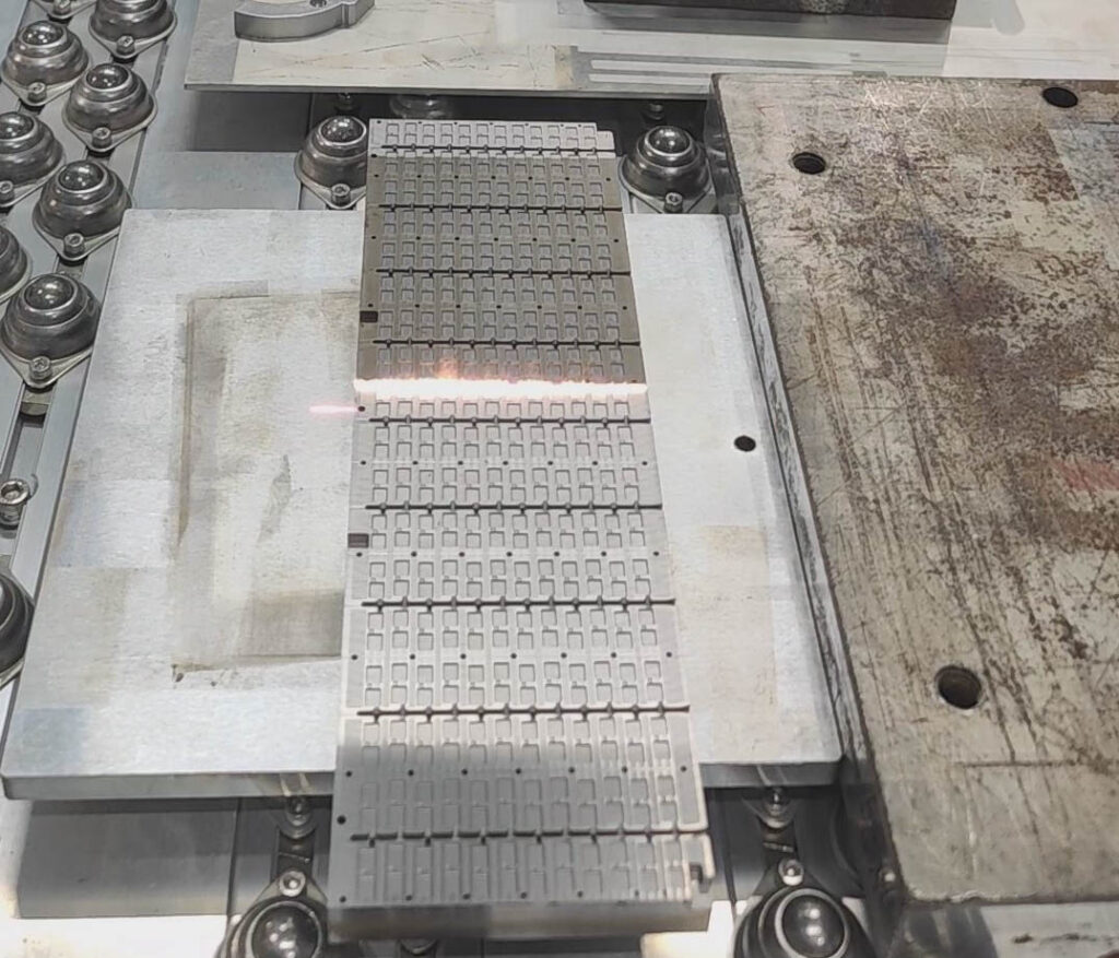
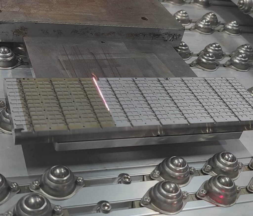
Laserreinigung Spezifische Anwendungen:
A. Epoxy Molding Compound Residue
This is the most common contaminant. During the transfer molding process, epoxy molding compound (EMC) forms hard, carbonized residue on mold parting surfaces, cavity corners, and ejector pinholes. These residues contain fillers such as silicon powder and are very stubborn.
B. Trennmittelakkumulation
Mold release agents used to ensure smooth demolding will continuously carbonize at high temperatures, forming a difficult-to-remove insulating film on the mold surface, affecting the surface quality and release performance of the molded product.
C. Inorganic Contaminants
Metal Flash: This arises from impurities in the molding compound or minor mold wear.
Oxide Layer: This is a surface oxide formed by long-term use of the mold in high-temperature environments.
Vorteil Abmessungen:
- Extreme Cleanliness, Zero Secondary Contamination: “Dry” cleaning eliminates any residual media. After cleaning, the mold surface is as clean as new, eliminating secondary contamination (such as chemical residue and media particles) introduced by cleaning at the source.
B. Improve chip product yield and reliability. By achieving 100% consistent, residue-free cleaning, this system completely eliminates defects such as poor chip bonding, warping, cracks, voids, and pitting caused by mold contamination, directly improving product yield and long-term reliability.
C. Meet absolute dust-free environment requirements. The equipment can be fully integrated into automated production lines and operate within a partial vacuum hood. Combined with a vacuum system, it meets the high-grade cleanroom requirements of chip manufacturing.


Modus empfehlen
Keine Ergebnisse gefunden.


